
With a stack of little flat wires known as nanosheets, IBM Investigate claims chips with quicker, smaller parts that use much less ability.
IBM Research
IBM Study has produced new chipmaking technological know-how it suggests will advance processors to the following level of circuitry miniaturization, general performance advancement and energy efficiency.
The new producing technological know-how, that includes parts termed nanosheets, raises chip general performance 45% or minimizes electric power use by 75% in comparison with the 1 used to make IBM server chips or Apple’s Apple iphone chips, the company stated Thursday. IBM expects the engineering to arrive in processors in 2024 or 2025, two generations further than the most innovative processes at the moment utilized by present day production chief Taiwan Semiconductor Production.
IBM is using the fundamental know-how that chip companies have employed for a long time: a cautiously arranged sample of mild beamed onto silicon wafers to etch patterns that become the facts-processing circuitry features named transistors. Steady refinements have enable chipmakers little by little shrink those transistors so that processors once utilised in place-sized mainframes can now electric power a smartwatch.
The new approach works by using two structures. The initially are nanosheets, the thin, flat wires that carry electrical present-day across the transistor. Next is a new structure for the gate, a element that switches present on or off. IBM works by using gate-all-close to technologies that totally surrounds every single nanosheet with the gate material to continue to keep electrical recent from leaking.
“We have the transistor unit to make it occur, and we are viewing the effectiveness improvements,” said Dario Gil, head of IBM Investigate, which licenses its chip know-how for producers to use. “The complete field is likely to use this transistor engineering.”
Chip development is important. Cutting ability utilization is significant for battery-limited cell products, as effectively as strengthening performance tends to make apps quicker and more effective. Shrinking transistors means a lot more circuitry for faster graphics, AI processing and other devoted hardware talents.
2nm producing approach
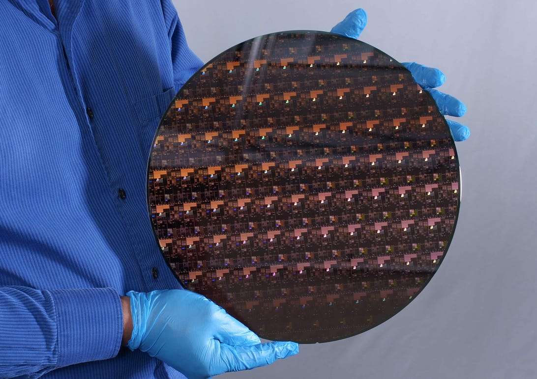
The company on Thursday showed off silicon wafers studded with rectangular chips utilizing the new approach. IBM Research is creating the exam chips at its semiconductor research facility in Albany, New York, a choice that will likely sit well with politicians keen to restore US chipmaking prowess.
Chipmakers refer to their production processes by the super-tiny dimension of nanometers, a billionth of a meter. A strand of DNA, for case in point, is 2nm broad. For chipmaking, a more compact nanometer selection suggests development in miniaturization although the phrases utilized nowadays are mainly labels somewhat than real measurements.
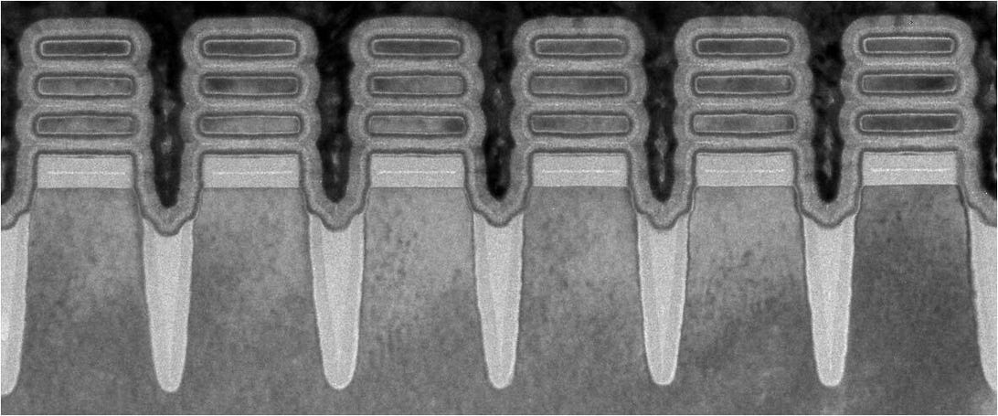
This photo displays a cross part of 6 transistors constructed with IBM’s nanosheet engineering. Every single has a stack of a few nanosheets that have electrical present. And with an strategy identified as gate all all over, each nanosheet is surrounded entirely by a gate, the transistor component that switches latest off and on. Present-day chips procedure facts using billions of this kind of transistors.
IBM Analysis
Modern most advanced production is TSMC’s 5-nanometer course of action. Considerably of the business nonetheless utilizes 7nm or previously processes. Subsequent in line is 3nm. IBM labels its new approach as 2nm.
Considering that we’re operating out of nanometers, it is not clear what labels will come subsequent, specially due to the fact the numbers are no more time true measurements.
Other chipmakers presently functioning on gate-all-all over
What isn’t clear is how the engineering will appear to market place considering that IBM no lengthier tends to make its very own processors.
The world’s a few key chipmakers — Intel, TSMC and Samsung — all have their own investigate applications and possible already are doing work on gate-all-around technological know-how, explained David Kanter, principal analyst at Serious Planet Insights. “Just about every major player obviously has programs for this.”
Samsung showed off its gate-all-all over technologies at a February conference, and Intel, like IBM, is operating on stacking multiple layers of nanosheets into each and every transistor.
IBM has partnerships with significant chipmakers, while. Samsung builds IBM server processors, and an IBM exploration alliance is component of new Intel Chief Govt Pat Gelsinger’s approach to turn around Intel’s yrs of difficulties.
Yet another complication for IBM will be proving its technological know-how performs outside the house of a lab in superior-quantity manufacturing, exactly where costs and consistency are crucial.
“For semiconductor producing, merely executing the R&D and proving it out is very a bit diverse than proving that it scales,” Kanter stated.